Six Layer Pcb With Lf-hasl And Gold Fingers Surface Treatment
Price:
Get Latest Price
In Stock
Product Overview
Key Features
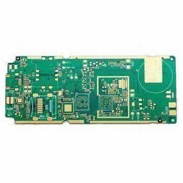
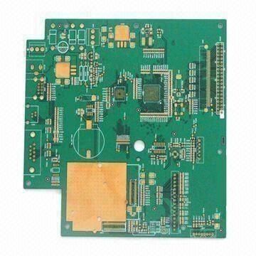
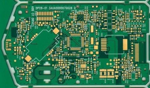
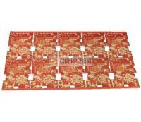
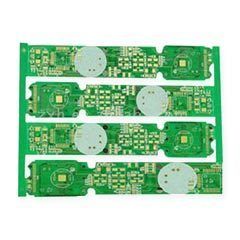
We are offering our customers a wide range of Six layer PCB with LF-HASL and Gold Fingers Surface Treatment, which are available following Specifications :-
Layer: 6
Base material: FR4
Copper thickness: 1oz
Minimum hole size: 0.3mm
Minimum line width: 0.35mm
Minimum line space: 0.4mm
Surface treatment: lead-free + gold fingers
Solder mask: blue
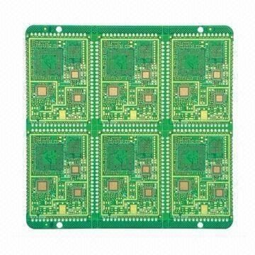
Panel array: four pieces in one panel
Profile: routing and v-cut
Packing: vacuum
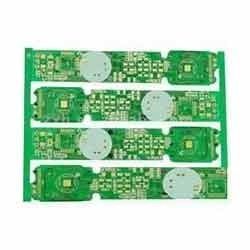
Layer: 6
Base material: FR4
Copper thickness: 1oz
Minimum hole size: 0.3mm
Minimum line width: 0.35mm
Minimum line space: 0.4mm
Surface treatment: lead-free + gold fingers
Solder mask: blue
Panel array: four pieces in one panel
Profile: routing and v-cut
Packing: vacuum
Company Details
Shenzhen 3c-technology Co.,Ltd, Established in 1998 at Shenzhen in Guangdong, is a leading service provider of Circuit Boards in China. Shenzhen 3c-technology Co.,Ltd is one of Trade India's verified and trusted names for listed services. With extensive experience in the field of Circuit Boards, Shenzhen 3c-technology Co.,Ltd has made a reputed name for itself in the market with satisfactory Double-Side PCB with Immersion Gold Surface Treatment, Double-layer Flexible PCB, Eight Layer ENIG HDI PCB, etc.
Focusing on a customer-centric approach, Shenzhen 3c-technology Co.,Ltd has a pan-India presence and caters to a huge consumer base throughout the country. Get Circuit Boards from Shenzhen 3c-technology Co.,Ltd at Trade India quality-assured services.
Focusing on a customer-centric approach, Shenzhen 3c-technology Co.,Ltd has a pan-India presence and caters to a huge consumer base throughout the country. Get Circuit Boards from Shenzhen 3c-technology Co.,Ltd at Trade India quality-assured services.
Business Type
Exporter, Service Provider, Supplier
Establishment
1998
Related Products
Gold Plated PCB - CNC Drilled, Multi-Layer Design | Hot Air Levelling & OSP Surface Finishing
Om Circuit Boards
Ghaziabad, Uttar Pradesh
Gold Plated PCB - Multi-Layered Gold Plated Circuit Boards | CNC Drilled, Hot Air Leveling, OSP Finishes
Chem-equip
Nashik, Maharashtra
Explore Related Categories


Seller Details
Shenzhen, Guangdong
Mr. Adam Chen
Address
Rm. 502, Xinbaosheng Bldg., 233 Xixiang Rd., Xixiang, Bao'an, Shenzhen, Guangdong, 518102, China
gold plating pcb in Shenzhen
Report incorrect details